Nanofoundry
Supporting the complete process from material characterization through device fabrication, culminating in device testing.
Equipped with a variety of advanced instruments that support research in material science and nanotechnology, the UND Nanofoundry has been funded by the State of North Dakota as a part of UND’s Space Education and Research Initiative. The investment is designed to enhance the university’s capabilities to pursue, secure and execute projects funded by both federal and private funding agencies. This initiative will generate extensive opportunities in research, training, and education for a broad range of colleges, schools, programs, faculty, and undergraduate and graduate students.
Virtual Video Tour
Faculty Expertise and Research Areas

- nuri.oncel@UND.edu
- 701.777.3529

- alena.kubatova@UND.edu
- 701.777.0348

- rajendra.dulal@UND.edu
- Office:701.777.3576 Cleanroom: 701.777.5500
- Tech Accelerator Room 1260 Grand Forks ND 58202-8367
Facility & Equipment Capabilities
The Nanofoundry is equipped with a variety of advanced instruments that support research in material science and nanotechnology. Some of these tools are used to study the properties of different materials, while others are designed to build small-scale electronic and optical devices.
ISO-6 (Class 1,000) Cleanroom
Located at UND Tech Accelerator
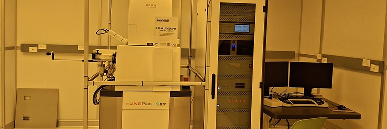
E-beam Lithography (Raith e-LINE Plus)
Uses a focused beam of electrons to create precise electronic and optical circuits on a surface.
Cryogenic 6-Probe Station (Lake Shore CRX-VF) with 2.5 T vertical magnetic field
Measures the electrical and optical properties of devices made using lithography techniques.
Maskless Aligner (Raith PicoMaster 100)
Uses a focused laser beam to create electronic and optical circuits on a surface.
Plasma Cleaner (PVA Ion Wave 10)
Primarily used for photoresist ashing and surface cleaning.
Stylus Profiler (Bruker DektakXT)
Designed to measure surface morphology with precision.
E-beam and Thermal Deposition System (Angstrom Engineering)
Utilized for the deposition of thin metal and oxide films.
Optical Microscope (Nikon Eclipse LV150N)
Used for characterizing surface morphology in detail.
Molecular Beam Epitaxy
- Located in Witmer Hall
- A highly controlled and precise method for fabricating crystalline semiconductor layers and other materials with atomic-level precision.
Scanning Transmission Electron Microscope (Talos F200X)
- Located in Witmer Hall
- Provides high-resolution images of nanomaterials at the atomic scale.
Size Exclusion Chromatography - Multi-Angle Light Scattering system (SEC-MALS)
- Located in Abbott Hall
- Separates complex mixtures, such as large molecules or colloidal particles, based on their size, typically in organic solvents.
Thermoelectric Measurement System (Linseis LSR-3)
- Located in Abbott Hall
- Measures the thermoelectric properties of materials.